Sign In | Join Free | My chinacomputerparts.com
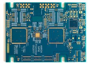
China Beijing Haina Lean Technology Co., Ltd logo
Beijing Haina Lean Technology Co., Ltd
Professional Manufactuer, Supply PCB Design,PCB Fabrication,PCB Assembly (PCBA ),Components Sourcing,Function Testing,Enclosure Assembly
Active Member

4 Years

Home > HDI PCB Board >

Buried Vias Enig Oem Pcb Board Multi-Layering 1oz Hdi

Beijing Haina Lean Technology Co., Ltd
Contact Now

Buried Vias Enig Oem Pcb Board Multi-Layering 1oz Hdi

  • 1
  • 2

Brand Name : HNL-PCBA

Model Number : PCB Assembly 012

Certification : ISO9001,IS16949, ISO14001,ROHS , UL, IPC-A , UL, QC080000

Place of Origin : CHINA

MOQ : 1 PC

Price : Negotiable

Payment Terms : T/T, Western Union, L/C, MoneyGram

Supply Ability : 10,000,000 Point /Day

Delivery Time : 1-7days

Packaging Details : ESD packaging with carton box

Product name : ENIG multi-layering 1oz HDI Printed Circuit Board

Material : FR-4/Normal Tg/High Tg/Low Dk/HF FR4/PTEE/PI

Copper thickness : 0.3oz...1oz 2oz ...6oz

Min. line spacing : 0.030mm,0.05mm ETC.

Min. hole size : 0.05mm, 0.1mm, 0.25mm, 0.1mm/4mil, 4mil, 0.02

Usage : OEM Electronics,Circuit Board Assembly

Board thickness : 0.3mm,,,1.6mm,,,3.5mm

solder mask : Green. Black. Red. Yellow. White. Blue etc.; custom

Type : buried vias and through vias

Surface Finishing : ENEPING /ENIG /HASL /FINGER GOLD/IMMERSION TIN/SELECTIVE THICK GOLD

Contact Now

ENIG Multi-Layering 1oz HDI Printed Circuit Board

HDI PCB Board Introduction

High Density Interconnection (HDI) PCB is a kind of (technology) for the production of printed circuit boards. It is a circuit board with relatively high circuit distribution density using micro blind via and buried via technology. Due to the continuous development of technology and the electrical requirements for high-speed signals, the circuit board must provide impedance control with AC characteristics, high-frequency transmission capability, and reduce unnecessary radiation (EMI). Adopting the structure of Stripline and Microstrip, multi-layering becomes a necessary design. In order to reduce the quality problem of signal transmission, insulating materials with low dielectric constant and low attenuation rate are used. In order to meet the miniaturization and arraying of electronic components, the density of circuit boards is constantly increasing to meet the demand.


PCB (Printed circuit board) is the most import role in the Electronic time, the electronic products which we can think of will need the PCB board, We are manufacture with year's experience in PCB & PCBA solutions .

PCB CAPABILITIES

FACTORY CAPABILITIES
No. Items 2019 2020
1 HDI Capabilities HDI ELIC (4+2+4) HDI ELIC(5+2+5)
2 Max layer count 32L 36L
3 Board Thickness Core thickness 0.05mm-1.5mm ,Fineshed board thickness 0.3-3.5mm Core thickness 0.05mm-1.5mm ,Fineshed board thickness 0.3-3.5mm
4 Min.Hole Size Laser 0.075mm Laser 0.05mm
Mechnical 0.15mm Mechnical 0.15mm
5 Min Line Width/Space 0.035mm/0.035mm 0.030mm/0.030mm
6 Copper Thickness 1/3oz-4oz 1/3oz-6oz
7 Size Max Panel size 700x610mm 700x610mm
8 Registration Accuracy +/-0.05mm +/-0.05mm
9 Routing Accuracy +/-0.075mm +/-0.05mm
10 Min.BGA PAD 0.15mm 0.125mm
11 Max Aspect Ratio 10:1 10:1
12 Bow and Twist 0.50% 0.50%
13 Impedance Control Tolerance +/-8% +/-5%
14 Daily Output 3,000m2 (Max capacity of equipment) 4,000m2 (Max capacity of equipment)
15 Surface Finishing ENEPING /ENIG /HASL /FINGER GOLD/IMMERSION TIN/SELECTIVE THICK GOLD
16 Raw Material FR-4/Normal Tg/High Tg/Low Dk/HF FR4/PTEE/PI

The types of HDI PCB


1.through vias from surface to surface,
2.with buried vias and through vias,
3.two or more HDI layer with through vias,
4.passive substrate with no electrical connection,
5.coreless construction using layer pairs
6.alternate constructions of coreless constructions using layer pairs.

HDI (High Density Interconnection) circuit boards usually include laser blind vias and mechanical blind vias; general through buried vias, blind vias, stacked vias, staggered vias, cross blind buried, through vias, blind via filling plating, fine line small gaps, The technology of realizing the conduction between the inner and outer layers by processes such as micro-holes in the disk, usually the diameter of the blind buried is not more than 6 mils.

Buried Vias Enig Oem Pcb Board Multi-Layering 1oz Hdi

Work flow for HDI

Board Cut - Inner Wet film -DES - AOI - Brown Oxido - Outer Layer Press - Out Layer Lamination - X-RAY & Rounting - Copper reduce & brown oxide - Laser Drilling - Drilling - Desmear PTH - Panel plating - Outer Layer dry film - Etching - AOI- Impedance Testing - S/M Pluged hole - Solder Mask - Component Mark - Impedance testing - Immersion Gold -V-cut - Routing - Electrical Test - FQC - FQA -Package -Shipment

Buried Vias Enig Oem Pcb Board Multi-Layering 1oz Hdi

Similar products

Buried Vias Enig Oem Pcb Board Multi-Layering 1oz Hdi

Buried Vias Enig Oem Pcb Board Multi-Layering 1oz Hdi

HDI PCB Board Application Field

Our PCB are widely used in communication equipment, industrial control, consumer electronics, medical equipment, aerospace, light-emitting diode lighting, automotive electronics etc.

Workshop

Buried Vias Enig Oem Pcb Board Multi-Layering 1oz Hdi

Buried Vias Enig Oem Pcb Board Multi-Layering 1oz Hdi

Common packaging

1.PCB: Vacuum packaging with carton box
2.PCBA: ESD packaging with carton box

Buried Vias Enig Oem Pcb Board Multi-Layering 1oz Hdi

Our advantage

1.Service value

Independent quotation system to quickly serve the market

2.PCB manufacturing

High-tech PCB and PCB assembly production line

3.Material purchasing

A team of experienced electronic component procurement engineers

4.SMT post soldering

Dust-free workshop, high-end SMT patch processing

Buried Vias Enig Oem Pcb Board Multi-Layering 1oz Hdi


Product Tags:

buried vias oem pcb board


enig oem pcb board


high density interconnect hdi pcb

      
China Buried Vias Enig Oem Pcb Board Multi-Layering 1oz Hdi factory

Buried Vias Enig Oem Pcb Board Multi-Layering 1oz Hdi Images

Inquiry Cart 0
Send your message to this supplier
 
*From:
*To: Beijing Haina Lean Technology Co., Ltd
*Subject:
*Message:
Characters Remaining: (0/3000)